This project focused on the design of a 8 bit (1 byte) Static Random Access Memory having serial input facility and also a differential voltage sense amplifier for noise robust read operation of the memory designed, using 180nm CMOS technology.This project was submitted as the endsem examination project for the course EE311- VLSI Laboratory
A bit of theory-
Static Random Access Memory (Static RAM or SRAM) is a type of RAM that holds data in a static form, that is, as long as the memory has power. There are two key features to SRAM which set it out against other types of memory that are available:
A 6T CMOS SRAM cell is the most popular SRAM cell due to its superior robustness, low power and low-voltage operation. Therefore, we will discuss its operation and design in greater detail. An SRAM cell must be designed such that it provides a non-destructive read operation and a reliable write operation
6T CMOS SRAM CELL:
A bit of theory-
Static Random Access Memory (Static RAM or SRAM) is a type of RAM that holds data in a static form, that is, as long as the memory has power. There are two key features to SRAM which set it out against other types of memory that are available:
- The data is held statically: this means that the data is held in the semiconductor memory without the need to be refreshed as long as the power is applied to the memory.
- SRAM is a form of random access memory : a random access memory is one in which the locations in the semiconductor memory can be written to or read from in any order, regardless of the last memory location that was accessed.
A 6T CMOS SRAM cell is the most popular SRAM cell due to its superior robustness, low power and low-voltage operation. Therefore, we will discuss its operation and design in greater detail. An SRAM cell must be designed such that it provides a non-destructive read operation and a reliable write operation
6T CMOS SRAM CELL:

6T SRAM Cell (which stores one binary bit ) has six Transistors comprising of two Cross-Coupled Inverters and two Access Transistors. In this format the circuit has two states, and these equate to the logical “0” and “1” states. In addition to the four transistors in the basic memory cell, and additional two transistors are required to control the access to the memory cell during the read and write operations. This makes a total of six transistors, making what is termed a 6T memory cell.
Sense amplifiers (SA):
These are an important component in memory design. The choice and design of a SA defines the robustness of bit line sensing, impacting the read speed and power. The primary function of a SA in SRAMs is to amplify a small analog differential voltage developed on the bit lines by a read-accessed cell to the full swing digital output signal thus greatly reducing the time required for a read operation. Since SRAMs do not feature data refresh after sensing, the sensing operation must be non destructive, as opposed to the destructive sensing of a DRAM cell. A SA allows the storage cells to be small, since each individual cell need not fully discharge the bit line.
The project consisted of various blocks (SIPO circuit, decoder, 6T SRAM, multiplexer, Sense Amplifier) that we designed independently and later integrated together to build a 1 byte SRAM with sense amplifier. Following is a schematic of the project -
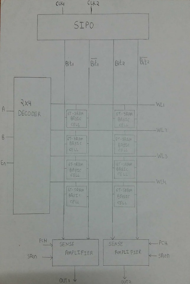
Following is a small collection of the schematic and layouts of the individual components as built for the project:
Please find below the final report of the project, which explains in detail the ideology for the construction of each component, working of each component aided with timing diagram, the interconnection between the sub-parts and the working of the final circuit as desired explained using timing diagrams(for both schematic and layout).
